- 您现在的位置:买卖IC网 > Sheet目录317 > C8051T610DB24 (Silicon Laboratories Inc)DAUGHTER BOARD T610 24QFN SOCKET
�� �
�
�C8051T610/1/2/3/4/5/6/7�
�21.2.� Assigning� Port� I/O� Pins� to� Analog� and� Digital� Functions�
�Port� I/O� pins� can� be� assigned� to� various� analog,� digital,� and� external� interrupt� functions.� The� Port� pins�
�assigned� to� analog� functions� should� be� configured� for� analog� I/O,� and� Port� pins� assigned� to� digital� or� exter-�
�nal� interrupt� functions� should� be� configured� for� digital� I/O.�
�21.2.1.� Assigning� Port� I/O� Pins� to� Analog� Functions�
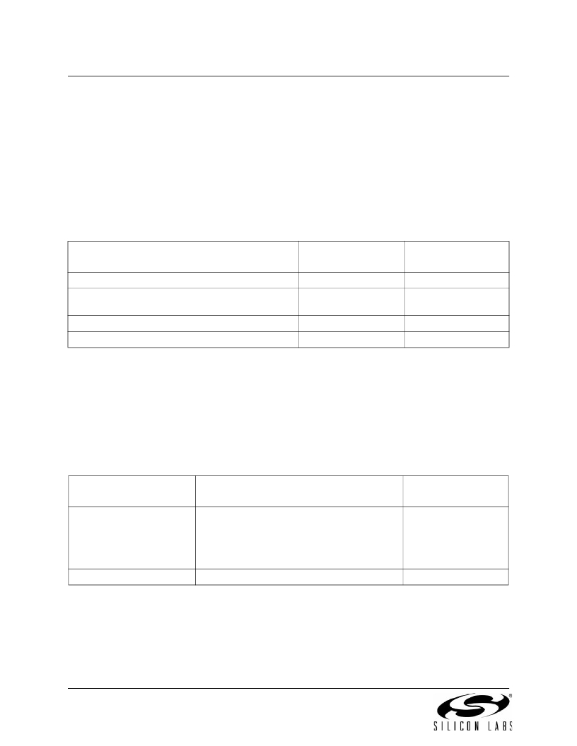
�Table� 21.1� shows� all� available� analog� functions� that� require� Port� I/O� assignments.� Port� pins� selected� for�
�these� analog� functions� should� have� their� corresponding� bit� in� PnSKIP� set� to� 1.� This� reserves� the� pin�
�for� use� by� the� analog� function� and� does� not� allow� it� to� be� claimed� by� the� Crossbar.� Table� 21.1� shows� the�
�potential� mapping� of� Port� I/O� to� each� analog� function.�
�Table� 21.1.� Port� I/O� Assignment� for� Analog� Functions�
�Analog� Function�
�ADC� Input�
�Comparator� Inputs�
�Voltage� Reference� (VREF0)�
�External� Oscillator� in� RC� or� C� Mode� (EXTCLK)�
�Potentially� Assignable�
�Port� Pins�
�P1.0–P3.4�
�P1.0–P2.7�
�P0.0�
�P0.3�
�SFR(s)� used� for�
�Assignment�
�AMX0P,� PnSKIP�
�CPT0MX,� CPT1MX,�
�PnSKIP�
�REF0CN,� PnSKIP�
�OSCXCN,� PnSKIP�
�21.2.2.� Assigning� Port� I/O� Pins� to� Digital� Functions�
�Any� Port� pins� not� assigned� to� analog� functions� may� be� assigned� to� digital� functions� or� used� as� GPIO.� Most�
�digital� functions� rely� on� the� Crossbar� for� pin� assignment;� however,� some� digital� functions� bypass� the�
�Crossbar� in� a� manner� similar� to� the� analog� functions� listed� above.� Port� pins� used� by� these� digital� func-�
�tions� and� any� Port� pins� selected� for� use� as� GPIO� should� have� their� corresponding� bit� in� PnSKIP� set�
�to� 1.� Table� 21.2� shows� all� available� digital� functions� and� the� potential� mapping� of� Port� I/O� to� each� digital�
�function.�
�Table� 21.2.� Port� I/O� Assignment� for� Digital� Functions�
�Digital� Function�
�UART0,� SPI0,� SMBus,� CP0,�
�CP0A,� CP1,� CP1A,�
�SYSCLK,� PCA0� (CEX0-4�
�and� ECI),� T0� or� T1.�
�Any� pin� used� for� GPIO�
�116�
�Potentially� Assignable� Port� Pins�
�Any� Port� pin� available� for� assignment� by� the�
�Crossbar.� This� includes� P0.0� -� P2.3� pins� which�
�have� their� PnSKIP� bit� set� to� 0.�
�Note:� The� Crossbar� will� always� assign� UART0�
�pins� to� P0.4� and� P0.5.�
�P0.0–P3.4�
�Rev� 1.1�
�SFR(s)� used� for�
�Assignment�
�XBR0,� XBR1�
�PnSKIP�
�发布紧急采购,3分钟左右您将得到回复。
相关PDF资料
C8051T630DB20
BOARD SOCKET DAUGHTER 20-QFN
CAN-100
BOARD EVAL RS232 100QFP
CANADAPT28
KIT ADAPTER CANDEMOBOARD 28PLCC
CAT24AA01WI-GT3
IC EEPROM SERIAL 1KB I2C 8SOIC
CAT24AA02WI-G
IC EEPROM SERIAL 2KB I2C 8SOIC
CAT24C01ZI-G
IC EEPROM SERIAL 1KB I2C 8MSOP
CAT24C03WI-G
IC EEPROM SERIAL 2KB I2C 8SOIC
CAT24C04ZI-G
IC EEPROM SERIAL 4KB I2C 8MSOP
相关代理商/技术参数
C8051T610DB28
功能描述:子卡和OEM板 C8051T610 Family Socket Daughtr Board RoHS:否 制造商:BeagleBoard by CircuitCo 产品:BeagleBone LCD4 Boards 用于:BeagleBone - BB-Bone - Open Source Development Kit
C8051T610DB32
功能描述:子卡和OEM板 C8051T610 Family Socket Daughtr Board RoHS:否 制造商:BeagleBoard by CircuitCo 产品:BeagleBone LCD4 Boards 用于:BeagleBone - BB-Bone - Open Source Development Kit
C8051T610DK
功能描述:开发板和工具包 - 8051 C8051T610 Series Development Kit RoHS:否 制造商:Silicon Labs 产品:Development Kits 工具用于评估:C8051F960, Si7005 核心: 接口类型:USB 工作电源电压:
C8051T610-GQ
功能描述:8位微控制器 -MCU 16KB 10ADC 32Pin MCU RoHS:否 制造商:Silicon Labs 核心:8051 处理器系列:C8051F39x 数据总线宽度:8 bit 最大时钟频率:50 MHz 程序存储器大小:16 KB 数据 RAM 大小:1 KB 片上 ADC:Yes 工作电源电压:1.8 V to 3.6 V 工作温度范围:- 40 C to + 105 C 封装 / 箱体:QFN-20 安装风格:SMD/SMT
C8051T610-GQR
功能描述:8位微控制器 -MCU 16KB 10ADC 32Pin MCU RoHS:否 制造商:Silicon Labs 核心:8051 处理器系列:C8051F39x 数据总线宽度:8 bit 最大时钟频率:50 MHz 程序存储器大小:16 KB 数据 RAM 大小:1 KB 片上 ADC:Yes 工作电源电压:1.8 V to 3.6 V 工作温度范围:- 40 C to + 105 C 封装 / 箱体:QFN-20 安装风格:SMD/SMT
C8051T611-GM
功能描述:8位微控制器 -MCU 16KB 10ADC 28Pin MCU RoHS:否 制造商:Silicon Labs 核心:8051 处理器系列:C8051F39x 数据总线宽度:8 bit 最大时钟频率:50 MHz 程序存储器大小:16 KB 数据 RAM 大小:1 KB 片上 ADC:Yes 工作电源电压:1.8 V to 3.6 V 工作温度范围:- 40 C to + 105 C 封装 / 箱体:QFN-20 安装风格:SMD/SMT
C8051T611-GMR
功能描述:8位微控制器 -MCU 16KB 10ADC 28Pin MCU RoHS:否 制造商:Silicon Labs 核心:8051 处理器系列:C8051F39x 数据总线宽度:8 bit 最大时钟频率:50 MHz 程序存储器大小:16 KB 数据 RAM 大小:1 KB 片上 ADC:Yes 工作电源电压:1.8 V to 3.6 V 工作温度范围:- 40 C to + 105 C 封装 / 箱体:QFN-20 安装风格:SMD/SMT
C8051T612-GQ
功能描述:8位微控制器 -MCU 8KB 10ADC 32Pin MCU RoHS:否 制造商:Silicon Labs 核心:8051 处理器系列:C8051F39x 数据总线宽度:8 bit 最大时钟频率:50 MHz 程序存储器大小:16 KB 数据 RAM 大小:1 KB 片上 ADC:Yes 工作电源电压:1.8 V to 3.6 V 工作温度范围:- 40 C to + 105 C 封装 / 箱体:QFN-20 安装风格:SMD/SMT